- 您现在的位置:买卖IC网 > Sheet目录985 > ISLA224IR72EV1Z (Intersil)BOARD EVALUATION FOR ISLA224P
�� �
�
�ISLA224P�
�CSB� STALLING�
�CSB�
�SCLK�
�SDIO�
�INSTRUCTION/ADDRESS�
�DATA� WORD� 1�
�DATA� WORD� 2�
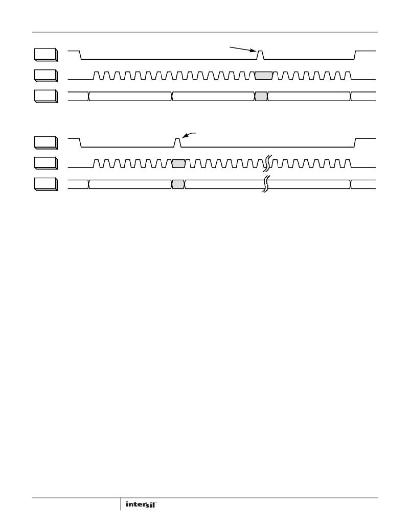
�FIGURE� 42.� 2-BYTE� TRANSFER�
�LAST� LEGAL�
�CSB�
�SCLK�
�CSB� STALLING�
�SDIO�
�INSTRUCTION/ADDRESS�
�DATA� WORD� 1�
�DATA� WORD� N�
�FIGURE� 43.� N-BYTE� TRANSFER�
�Serial� Peripheral� Interface�
�A� serial� peripheral� interface� (SPI)� bus� is� used� to� facilitate�
�configuration� of� the� device� and� to� optimize� performance.� The� SPI�
�bus� consists� of� chip� select� (CSB),� serial� clock� (SCLK)� serial� data�
�output� (SDO),� and� serial� data� input/output� (SDIO).� The� maximum�
�SCLK� rate� is� equal� to� the� A/D� sample� rate� (f� SAMPLE� )� divided� by� 32�
�for� write� operations� and� f� SAMPLE� divided� by� 132� for� reads.� At�
�f� SAMPLE� =� 250MHz,� maximum� SCLK� is� 15.63MHz� for� writing� and�
�3.79MHz� for� read� operations.� There� is� no� minimum� SCLK� rate.�
�The� following� sections� describe� various� registers� that� are� used� to�
�configure� the� SPI� or� adjust� performance� or� functional� parameters.�
�Many� registers� in� the� available� address� space� (0x00� to� 0xFF)� are�
�not� defined� in� this� document.� Additionally,� within� a� defined�
�register� there� may� be� certain� bits� or� bit� combinations� that� are�
�reserved.� Undefined� registers� and� undefined� values� within� defined�
�registers� are� reserved� and� should� not� be� selected.� Setting� any�
�reserved� register� or� value� may� produce� indeterminate� results.�
�SPI� Physical� Interface�
�The� serial� clock� pin� (SCLK)� provides� synchronization� for� the� data�
�transfer.� By� default,� all� data� is� presented� on� the� serial� data�
�input/output� (SDIO)� pin� in� three-wire� mode.� The� state� of� the� SDIO�
�pin� is� set� automatically� in� the� communication� protocol�
�(described� in� the� following).� A� dedicated� serial� data� output� pin�
�(SDO)� can� be� activated� by� setting� 0x00[7]� high� to� allow� operation�
�in� four-wire� mode.�
�The� SPI� port� operates� in� a� half� duplex� master/slave�
�configuration,� with� the� ISLA224P25� functioning� as� a� slave.�
�Multiple� slave� devices� can� interface� to� a� single� master� in�
�three-wire� mode� only,� since� the� SDO� output� of� an� unaddressed�
�device� is� asserted� in� four� wire� mode.�
�The� chip-select� bar� (CSB)� pin� determines� when� a� slave� device� is�
�being� addressed.� Multiple� slave� devices� can� be� written� to�
�concurrently,� but� only� one� slave� device� can� be� read� from� at� a�
�given� time� (again,� only� in� three-wire� mode).� If� multiple� slave�
�24�
�devices� are� selected� for� reading� at� the� same� time,� the� results� will�
�be� indeterminate.�
�The� communication� protocol� begins� with� an� instruction/address�
�phase.� The� first� rising� SCLK� edge� following� a� high-to-low�
�transition� on� CSB� determines� the� beginning� of� the� two-byte�
�instruction/address� command;� SCLK� must� be� static� low� before�
�the� CSB� transition.� Data� can� be� presented� in� MSB-first� order� or�
�LSB-first� order.� The� default� is� MSB-first,� but� this� can� be� changed�
�by� setting� 0x00[6]� high.� Figures� 38� and� 39� show� the� appropriate�
�bit� ordering� for� the� MSB-first� and� LSB-first� modes,� respectively.� In�
�MSB-first� mode,� the� address� is� incremented� for� multi-byte�
�transfers,� while� in� LSB-first� mode� it’s� decremented.�
�In� the� default� mode,� the� MSB� is� R/W,� which� determines� if� the�
�data� is� to� be� read� (active� high)� or� written.� The� next� two� bits,� W1�
�and� W0,� determine� the� number� of� data� bytes� to� be� read� or�
�written� (see� Table� 4).� The� lower� 13� bits� contain� the� first� address�
�for� the� data� transfer.� This� relationship� is� illustrated� in� Figure� 40,�
�and� timing� values� are� given� in� “Switching� Specifications”� on�
��After� the� instruction/address� bytes� have� been� read,� the�
�appropriate� number� of� data� bytes� are� written� to� or� read� from� the�
�A/D� (based� on� the� R/W� bit� status).� The� data� transfer� will�
�continue� as� long� as� CSB� remains� low� and� SCLK� is� active.� Stalling�
�of� the� CSB� pin� is� allowed� at� any� byte� boundary�
�(instruction/address� or� data)� if� the� number� of� bytes� being�
�transferred� is� three� or� less.� For� transfers� of� four� bytes� or� more,�
�CSB� is� allowed� to� stall� in� the� middle� of� the� instruction/address�
�bytes� or� before� the� first� data� byte.� If� CSB� transitions� to� a� high�
�state� after� that� point� the� state� machine� will� reset� and� terminate�
�the� data� transfer.�
�FN7570.1�
�November� 30,� 2012�
�发布紧急采购,3分钟左右您将得到回复。
相关PDF资料
ISPTPKIT
SCREW KIT TAMPER RESISTANT 9PCS
ITCSN-0400-25-U
HEATSHRINK ITCSN 2/5" X 25'
JC2AF-TM-DC24V-F
RELAY GEN PURPOSE DPST 10A 24V
JJM1A-12V
RELAY AUTOMOTIVE SPST 20A 12V
JM1AN-ZTM-DC5V-F
RELAY GEN PURPOSE SPST 20A 5V
JQ1P-18V-F
RELAY GEN PURPOSE SPDT 10A 18V
JS1-F-6V-F
RELAY GEN PURPOSE SPDT 10A 6V
JSM1-9V-5
RELAY AUTOMOTIVE SPDT 15A 9V
相关代理商/技术参数
ISLA224P
制造商:INTERSIL 制造商全称:Intersil Corporation 功能描述:Dual 14-Bit, 250MSPS/200MSPS/130MSPS ADC
ISLA224P12
制造商:INTERSIL 制造商全称:Intersil Corporation 功能描述:High Performance Dual 14-Bit, 125MSPS ADC
ISLA224P12IRZ
制造商:Intersil Corporation 功能描述:DUAL 14-BIT 125MSPS UNBUFFERED INPUT, 72-PIN - Trays 制造商:Intersil Corporation 功能描述:IC ADC 14BIT SPI/SRL 125M 48QFN 制造商:Intersil 功能描述:Dual 14-Bit 125MSPS Unbuffered Input, 72
ISLA224P13
制造商:INTERSIL 制造商全称:Intersil Corporation 功能描述:Dual 14-Bit, 250MSPS/200MSPS/130MSPS ADC
ISLA224P13IRZ
制造商:Intersil Corporation 功能描述:DUAL 14-BIT 130MSPS UNBUFFERED INPUT, 72-PIN - Trays 制造商:Intersil Corporation 功能描述:IC ADC 14BIT SRL/SPI 72QFN 制造商:Intersil 功能描述:DL 14-BIT 130MSPS UNBUFRED INPUT 72PIN
ISLA224P20
制造商:INTERSIL 制造商全称:Intersil Corporation 功能描述:Dual 14-Bit, 250MSPS/200MSPS/130MSPS ADC
ISLA224P20IRZ
制造商:Intersil Corporation 功能描述:DUAL 14-BIT 200MSPS UNBUFFERED INPUT, 72-PIN - Trays 制造商:Intersil Corporation 功能描述:IC ADC 14BIT SRL/SPI 72QFN 制造商:Intersil 功能描述:DL 14-BIT 200MSPS UNBUFRED INPUT 72PIN 制造商:Intersil Corporation 功能描述:IC, ADC, 14BIT; Resolution (Bits):14bit; Sampling Rate:200MSPS; Supply Voltage Type:Single; Supply Voltage Min:1.7V; Supply Voltage Max:1.9V; Supply Current:375mA; Digital IC Case Style:QFN; No. of Pins:72; Data Interface:SPI ;RoHS Compliant: Yes
ISLA224P25
制造商:INTERSIL 制造商全称:Intersil Corporation 功能描述:Dual 14-Bit, 250MSPS/200MSPS/130MSPS ADC